Design A Combinational Circuit That Generates Output As 1 Use K Map For Boolean Minimization
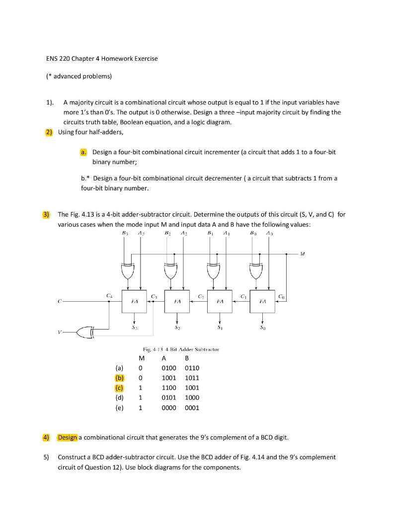
Solved Ens 220 Chapter 4 Homework Exercise Advanced Pro Chegg Com
L04 Combinational Logic
Q 4 4 Design A Combinational Circuit With Three Inputs And One Output A The Output Is 1 When Youtube
Solved 2 Design A Four Bit 2 S Complementer Combinationa Chegg Com
Solved Design A Combinational Circuit That Generates The 9 S C Chegg Com
Solved Design An Odd Parity Circuit This Is A Circuit That Ha Chegg Com

P a b ex nor c.
Design a combinational circuit that generates output as 1 use k map for boolean minimization.
Combinational Circuits Using Decoder Geeksforgeeks
Ch 4 Combinational Logic Circuits Ppt Download

Combinational Logic Logic Electronic Engineering Circuit
Digital Circuits K Map Method Tutorialspoint

1 Ee121 John Wakerly Lecture 4 Combinational Circuit Synthesis Abel Ppt Download
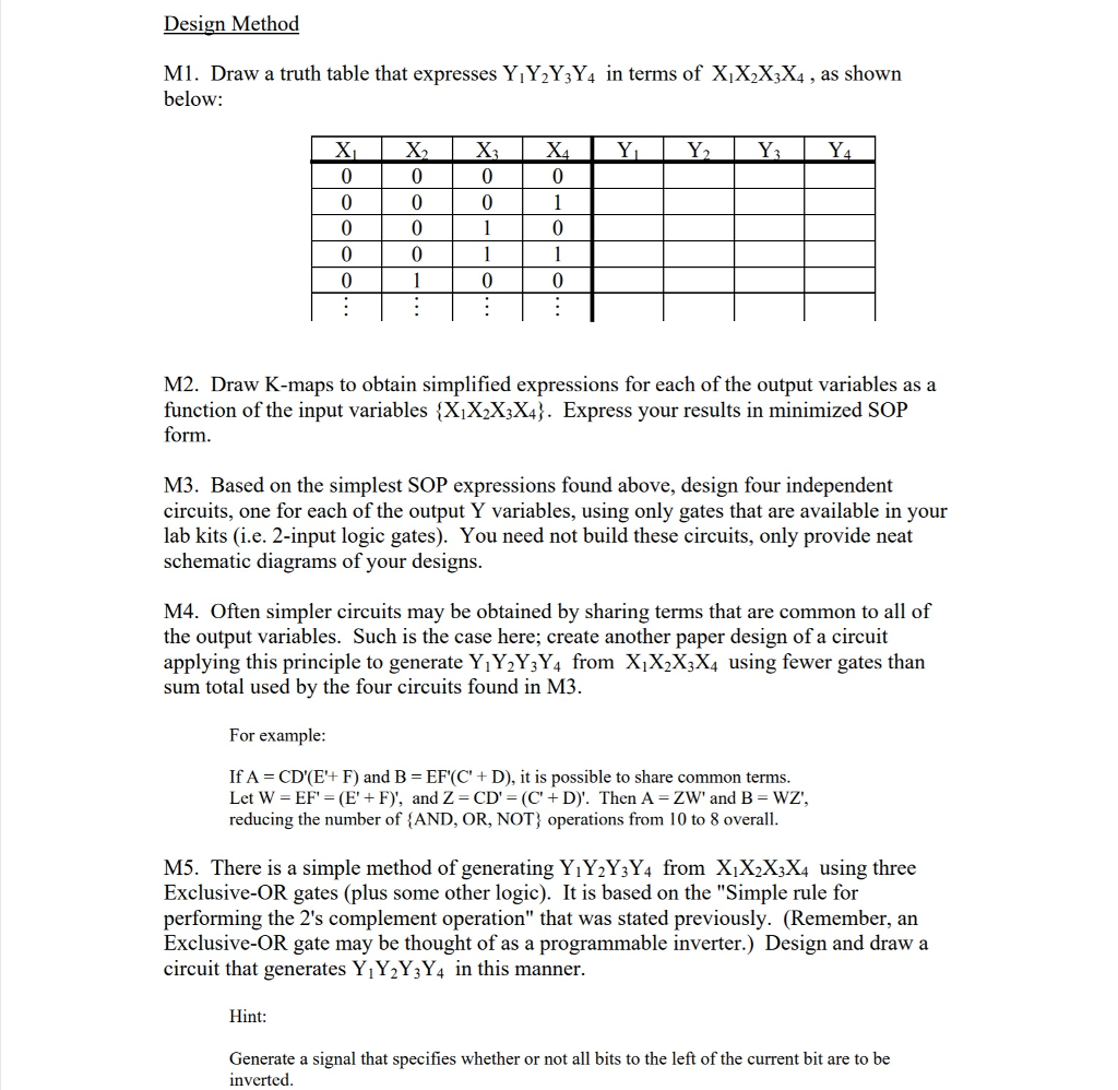
Solved Advanced Combinational Logic 2 S Complement Oper Chegg Com

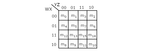
Pin On Mrmgate
How Could I Design A Logic Circuit That Counts The Number Of 1s In 3 Inputs A B C And Outputs A Two Bit Binary Number Representing That Count Of 1s Quora
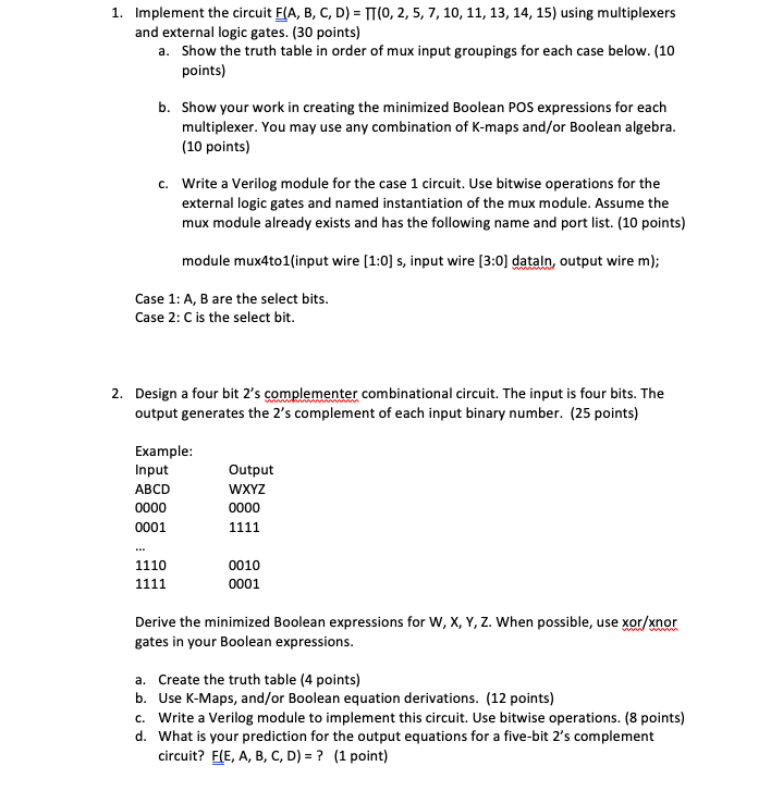
Solved 1 Implement The Circuit F A B C D 17 0 2 Chegg Com

Binary Logic And Gates Binary Logic Deals With Binary Variables I E Can Have Two Values 0 And 1 Binary Variables Can Undergo Three Basic Logical Ppt Download

Combinational Logic Circuits Using Logic Gates

Combinational Logic An Overview Sciencedirect Topics

Priority Encoder And Digital Encoder Tutorial

Introduction To Digital Logic Design Appendix A Of Co A Dr Farag Ppt Video Online Download

Chap 3 Chap 3 Combinational Logic Design Chap Combinational Circuits L Logic Circuits For Digital Systems Combinational Vs Sequential L Combinational Ppt Download
How To Design A Combinational Circuit With A Decoder To Accept A 3 Bit Number And Generate The Output Binary Number Equal To The Square Of The Input Number Quora
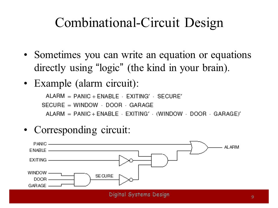
Digital Systems Design 1 Signal Expressions Multiply Out F X Y Z X Y Z X Z Y Z X Y Z Ppt Download
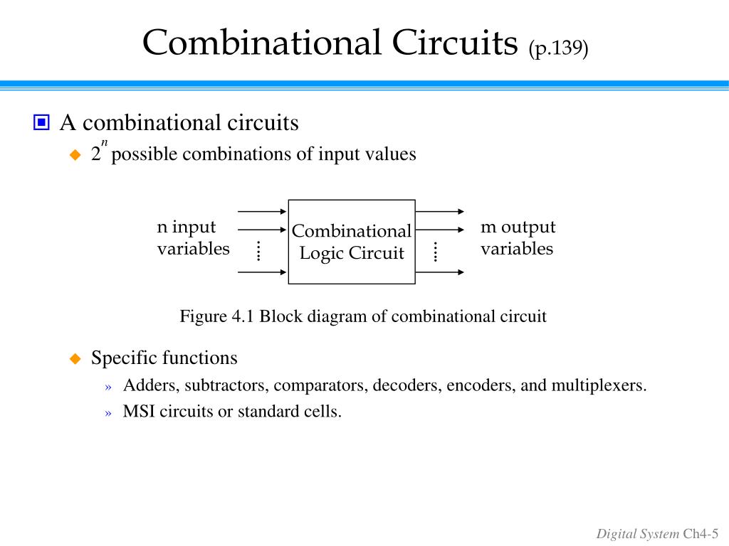
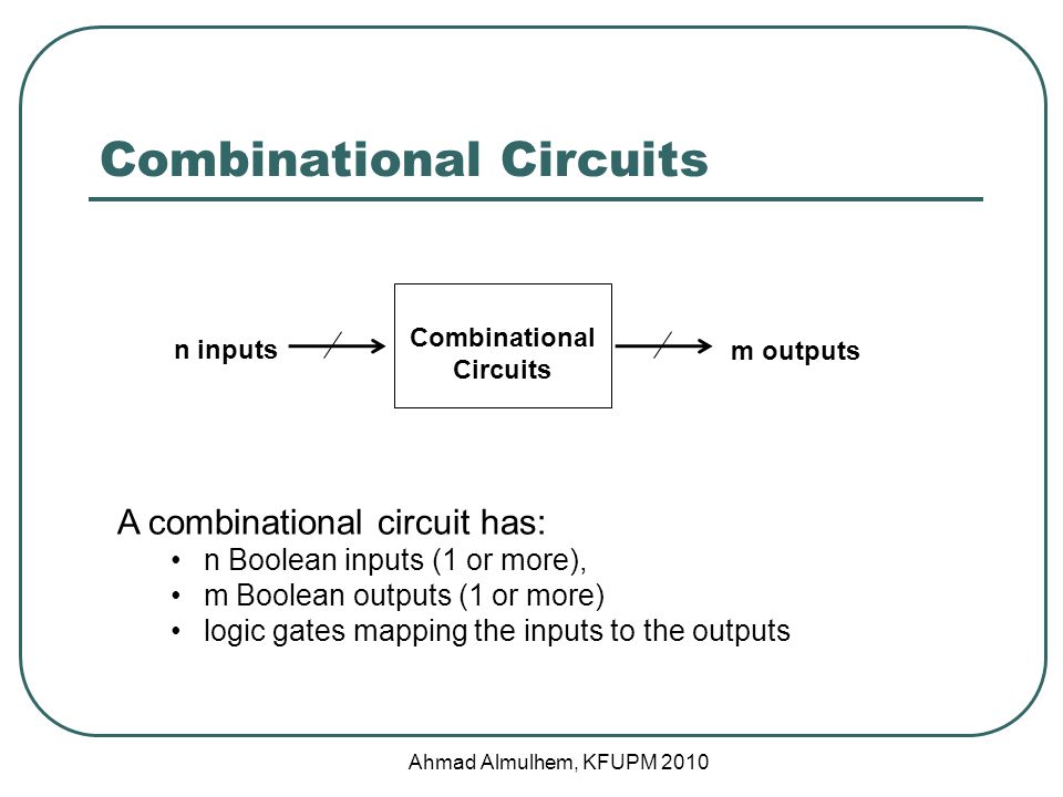
Ppt Chapter 4 Combinational Logic Powerpoint Presentation Free Download Id 4385910
Https Encrypted Tbn0 Gstatic Com Images Q Tbn 3aand9gctwfpfbf0ekbpk63pq8e9jykh7z6h5ez0q Radxdse88hiwcusz Usqp Cau

Sum Of Products Form An Overview Sciencedirect Topics
Https Ece Uwaterloo Ca Msachdev Ece223 Assignment4 Solution 3rd Edition Pdf

4 1 Annotated Slides 4 Combinational Logic Computation Structures Electrical Engineering And Computer Science Mit Opencourseware
Coe 202 Digital Logic Design Combinational Circuits Part 1 Ppt Download
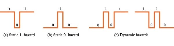
Hazards In Combinational Logic Technical Articles
Source : pinterest.com
