Cvd Graphene Copper Etching

Clean And Efficient Transfer Of Cvd Grown Graphene By Electrochemical Etching Of Metal Substrate Sciencedirect

Cvd Graphene Growth Transfer Ishigami Group Wiki

New Way To Make Cheap Graphene Thermoelectric Materials Material Science Nanotechnology

Chemical Etching Of Copper Foils For Single Layer Graphene Growth By Chemical Vapor Deposition Sciencedirect

Schematic Illustration For The Preparation Of Cvd Graphene Strips Download Scientific Diagram
Cvd Graphene
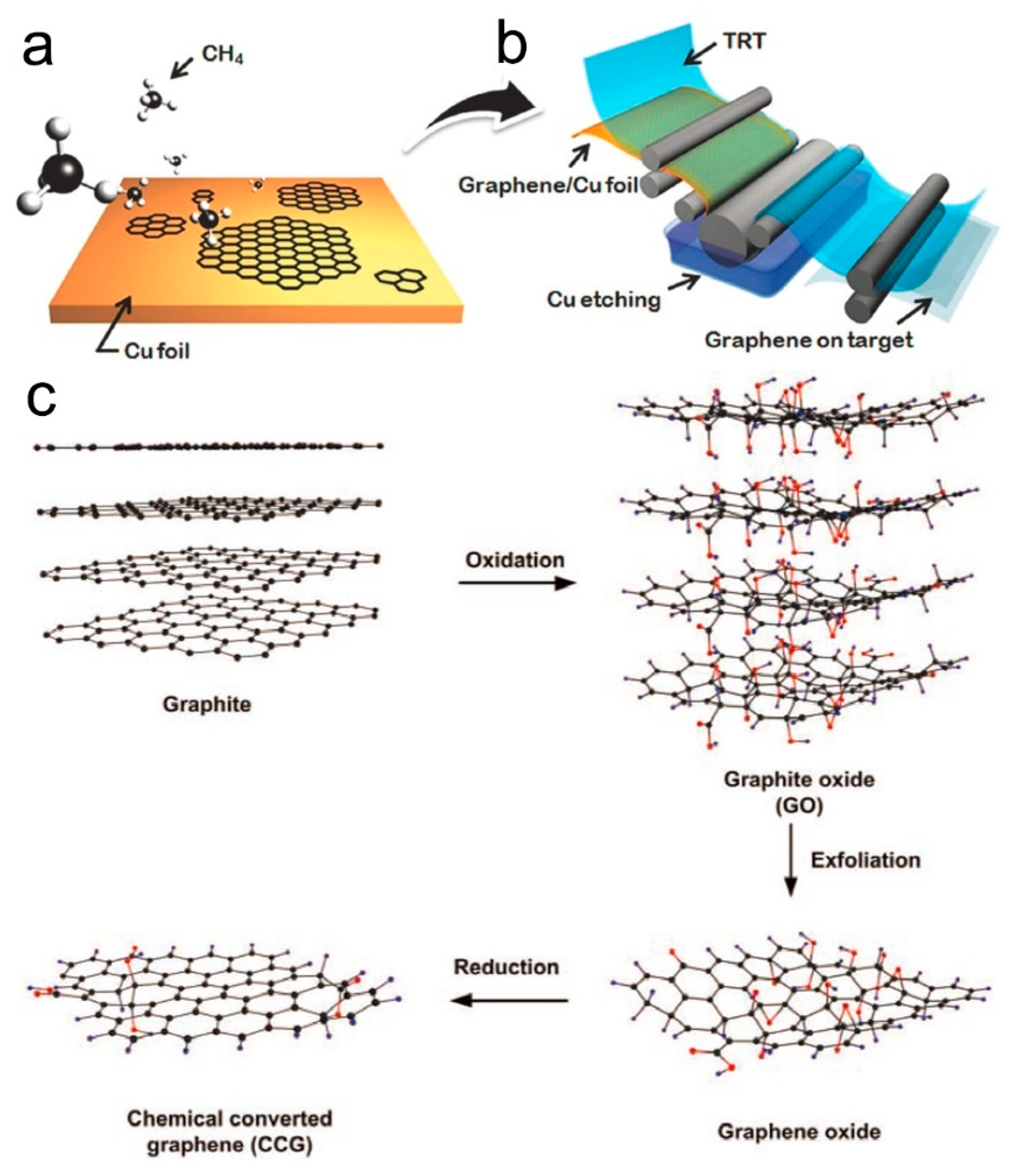
For the fecl 3 etchant we found that the average size of the.
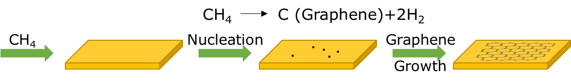
Cvd graphene copper etching.

Structure And Fabrication Process Of Cvd Grown Graphene On Pet Eva Download Scientific Diagram

Schematics Of The Transfer Process A Chemical Vapor Deposition Cvd Download Scientific Diagram

Monolayer Graphene Transfer Process To Polymeric Substrates A Download Scientific Diagram

Synthesis Based Application Of Graphene Nanotechnology Transistors Touch Screen

Schematic Showing In Situ Etching Process On Cvd Graphene Film For Download Scientific Diagram

Transfer Printing Of A Cvd Grown Graphene Monolayer The Process Download Scientific Diagram

Oil Boundary Approach For Sublimation Enabled Camphor Mediated Graphene Transfer Sciencedirect

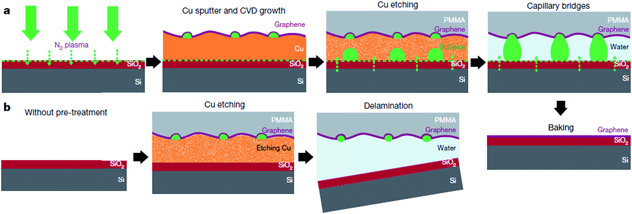
Synergistic Oxidation Of Cvd Graphene On Cu By Oxygen Plasma Etching Sciencedirect
Review Of The Synthesis Transfer Characterization And Growth Mechanisms Of Single And Multilayer Graphene Rsc Advances Rsc Publishing Doi 10 1039 C7ra00392g

Direct Observation Of Grain Boundaries In Graphene Through Vapor Hydrofluoric Acid Vhf Exposure Science Advances

Carbon Doped With Nitrogen Dramatically Improves Storage Capacity Of Supercapacitors Thermoelectric Materials Science Nanotechnology

Paraffin Enabled Graphene Transfer Nature Communications

Etching Controlled Growth Of Graphene Fragments On A Cu Surface A Download Scientific Diagram

A Schematic Of Cvd System For Graphene Growth B Schematic Of The Download Scientific Diagram

The Production Of Cu Nanoparticles On Large Area Graphene By Sputtering And In Flight Sintering Unlu 2017 Crystal Research And Technology Wiley Online Library

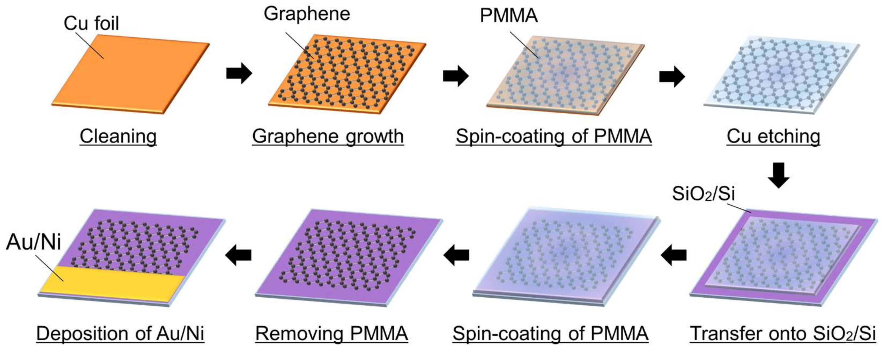
A I Schematic Process Flow For The Fabrication Of Cvd Graphene Download Scientific Diagram

Direct Transfer Process Of Ultra Large Area Graphene From Cu Foil To Download Scientific Diagram
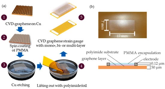
Sensors Free Full Text Strain Gauges Based On Cvd Graphene Layers And Exfoliated Graphene Nanoplatelets With Enhanced Reproducibility And Scalability For Large Quantities Html
Crystals Free Full Text Electrochemical Characterization Of Cvd Grown Graphene For Designing Electrode Biomolecule Interfaces Html

Progress And Challenges In Transfer Of Large Area Graphene Films Chen 2016 Advanced Science Wiley Online Library
Nanomaterials Free Full Text Recent Advances In Graphene Based Humidity Sensors Html
Http Iopscience Iop Org Article 10 1088 2053 1583 Aa69b5 Pdf

Optical Microscopic Image Of Copper Based Cvd Graphene On Sio 2 Si Download Scientific Diagram

The Porosity Of Graphene After Cvd Growth In The Presence Of An Download Scientific Diagram
Source : pinterest.com
